¶ Description
Sppice (Special Plate-on-Print Ion-Cooper Emissions) is our attempt at embedding electrically conductive elements on 3D printed parts. We envisioned a two-step process that can be executed at a relatively low cost using commodity tooling.
¶ Process
To embed electrical conductors in a part, we will use a electrolysis bath to deposit copper metal where it is needed. To achieve this, traces need to be painted using electrically conductive paint (or paste) in order to become an electrode.
The process is subdivided further into the electrolysis bath in two main parts: strike bath and layer thickening.
Strike bath is the first step, being composed of an aggressive plating process which strives to cover all of the printed traces in copper, making use of the electrical properties of the deposited layer. At this stage, we're using a low current (around 200mA).
The target is partially submerged in an initial solution that only contains copper sulfate and distilled water, allowing for local copper hydroxide deposition processes to take place on the top layer of the electrical trace.
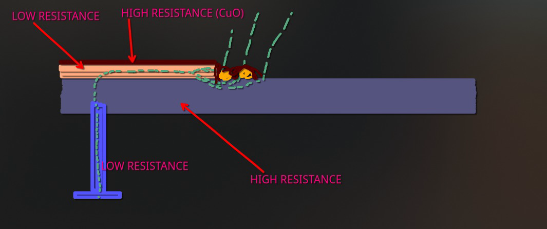
diagram showing a profile view of the plating process during strike bath
As it can be seen in the picture, there is a local hydroxide layer built on top of a thin, conductive copper layer. This process helps to lay out a initial layer of uniform conductor that prevents uneven deposition of bulk copper in the next stages.
The initial strike bath can be omitted if and only if the conductive substrate is on the order of tenths of an ohm.
Layer thickening is the second step, allowing for copper deposition under normal conditions. Sulphuric acid is added to the mix, preventing the firther deposition of copper hydroxide, creating the bulk conductive copper layer. At this stage, copper deposition happens at a very fast rate, trace resistance plummeting exponentially, electronics grade traces are being formed. The acid also allows for higher currents to be used, breaking unwanted OH bonds in the solution created by electrolisys.
| Diagram showing the copper deposition rate at different currents |
|---|
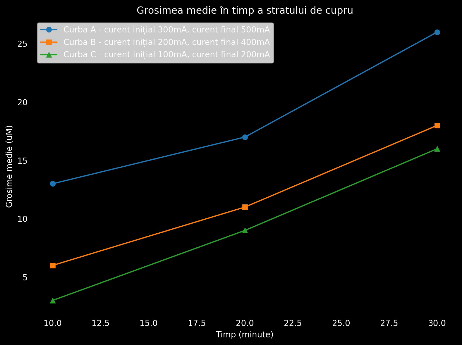 |
¶ Evaluating and maintaining normal copper deposition rate
The quality of the deposited copper depends on a few variables: current, quantity/existence of acid in the chemical bath and copper replacement rate, which remains almost constant throughout most of the plating process.
Lack of sulphuric acid in the solution will lead to porosity in the main copper layer, caused by the crystaline shape of copper hydroxide inside the layer.
Plating in the main bath at too high currents will outrun the acid's ability to break down hyrdoxide, and this can be observed as two symptoms:
- Crystal growth in the copper layer.
- Increase in voltage, caused by bad conductivity of copper hydroxide.
For our experiment, we have used a sensitive power source, capable of reading mV changes in the solution bath. After the strike bath is finished and we start adding the acid, we can start increasing the current to about 300-500 mA. it's important we monitor the voltage rate of change, rapid increases in voltage corresponding to hydroxide layer formation. A slow drop in voltage means the process is functioning and copper gets deposited correctly. As we have mentioned, resistance drops exponentially at this stage, final voltage readings corresponding to about a 0.1V.
it's recommended we use a heater to keep the temperature constant in the solution bath during most of the plating procedure. higher temperatures accelerate the process at low risks (compared to increasing the current).
For our purposes, we have decided to keep the temperature constant at about 40 degrees celsius. Higher temperatures can affect the way the sulphuric acid interacts with the rest of the environment, 40C being set at an optimal value.
Furthermore, voltage changes are a easy to measure way of evaluating and approximating deposition, finding the appropriate time at which to physically check layer thickness.
¶ Electrode paste deposition
To create an electrically conductive solid layer, we started off using very fine graphite powder and a volatile solvent (acetone). This approach yielded good deposition uniformity and low electrical resistance, but the layer is mechanically very fragile. The graphite layer will diffuse inside the electrolyte bath and the deposited copper will peel off very easily.
To mitigate these effects, we added a binder to our paste. We tested three acetone-soluble polymers and settled on ABS, which had the best properties for our project.
We also researched optimal drying conditions to evaporate the solvent. Tests showed that slower, cooler drying at about 55C prevents cracking of the paste layers from evaporation pressure.
| Binder | Resistance after 10 minutes | Resistance after 30 minutes | Change |
|---|---|---|---|
| ABS | 900 | 750 | -16.7% |
| ASA | 1150 | 1100 | -4.4% |
| HIPS | 1350 | 1190 | -12% |
Different concentrations of binder were tested for mechanical properties and electrical resistance. It was found that, at low binder concentrations (under 5%), electrical resistance is not significantly affected.
Overall electrical resistance can be greatly affected by the nature of the connection to the electrical wire:
- Alligator clips offer 2-6 small points of contact with a high pressure. Contact resistance is on the order of kOhms.
- A screw embedded inside the substrate, underneath the paste layer can give a few mm2 of good contact. Resistance is between 0 and 2 Ohms.
Because acetone dries quickly at room temperature, it is difficult to obtain a smooth application of the paste. To combat this, we have designed insets where paste is deposited. This allows for the plastic part to be lapped using sandpaper and also creates a smoother surface finish for the deposited copper.
¶ Preparing the target before plating
It's important that the surface of the target traces are cleaned of any grease, volatile substances that otherwise would impact adherence. This degreasing process is normally done using highly toxic industrial grade cyanides. We have used isopropyl alcohol to clean most of the traces, a better and safer approach.
¶ Electroplating Bath
To deposit copper onto conductive paste layer, we are using the electrolysis of copper (II) sulfate (CuSO4), which is readily available for agricultural use. A current-controlled power source is ideal because it will alow us to control the rate of deposition (mA/mm2) regardless of electrode contact resistance or other changing parameters.
It is very important for the metal anode contacts (wires, clips) to not come into contact with the electrolysis solution. Because of the higher resistance of the graphite paste (in comparison with pure copper or steel), failing to do so will leak most of the current trough the metal contact itself, bringing productive deposition of copper to a halt. To prevent this situation, we are routing anode contacts to the other side of the board using buried screws underneath the conductive paste. The board is partially submerged in the solution.
The rate of deposition is controlled by changing the outgoing current density trough the boundary of the paste. At higher currents, the Cu2+ ions are not replenished fast enough to carry the current, therefore water molecules are broken down into H2 and OH-. Hydroxide ions lead to the formation of unwanted Cu(OH)2, which can be spotted as green depositions around high-current areas. This phenomenon can be mitigated by adding a small amount of sulphuric acid (70g/L) which serves to oxidize the Cu(OH)2 back into CuSO4. The sulphuric acid also helps reduce the rate of Cu(OH)2 production by aiding with current carrying.
¶ Evaluating layer thickness
It's important that the electrode has contact points on top of the paste, outside the solution bath, the resistance of the traces being thus the parallel resistance of the copper layer in parallel with the graphite paint. once we get to the second plating stage, resistance will decrease rapidly in the copper layer, graphite resistance being overlooked.
¶ Proposed circuit
On our first try we have plated a simple circuit, composed of an led and a resistor in series connected to a 9v battery.
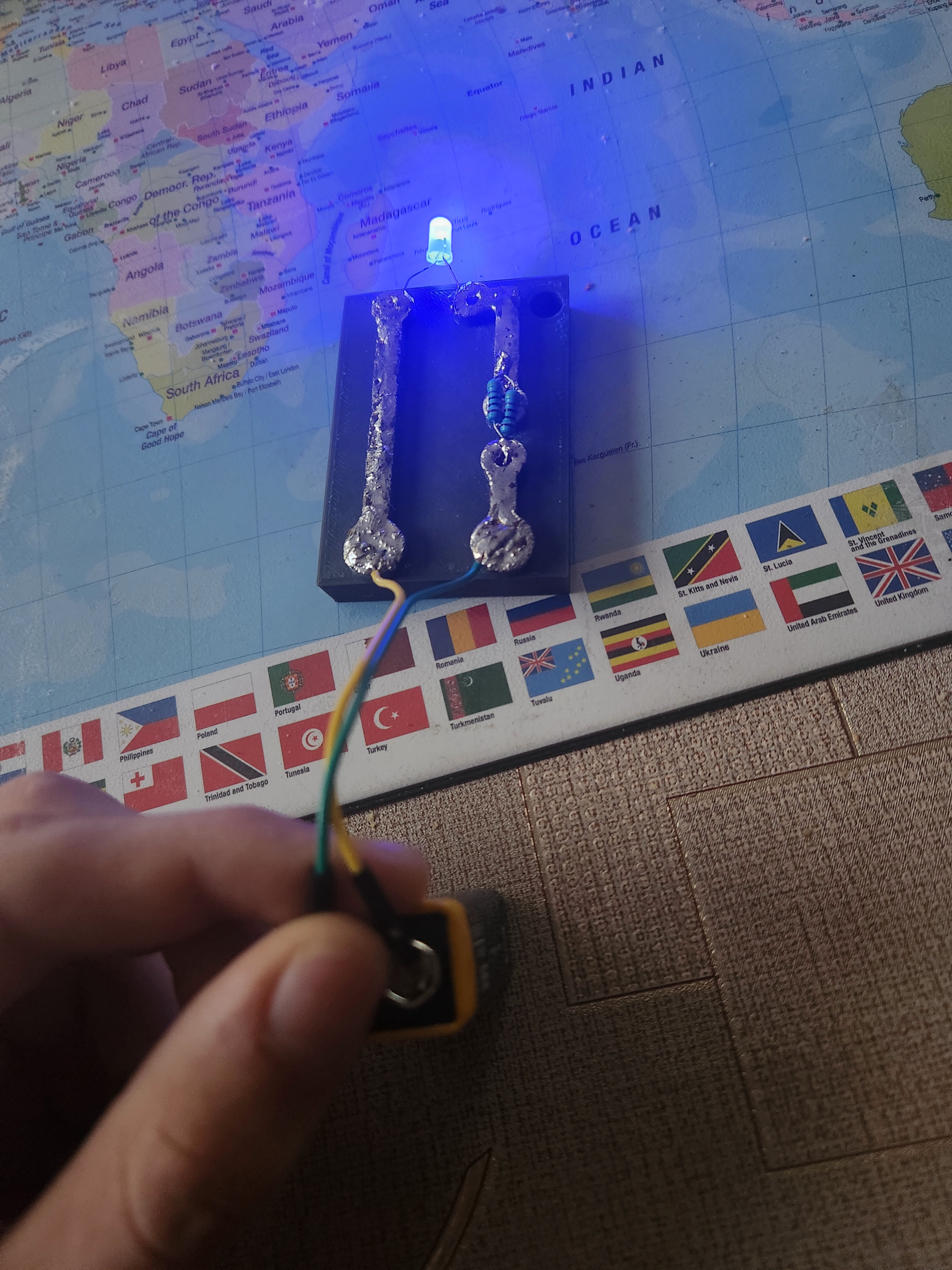 |
|---|
With this test, he have found out that the deposited copper layer has great porosity and absorption, enabling easy soldeing. Also, the plated traces as well as the graphite underneath act as heatsinks, therefore enabling soldering at temperatures that over the melting point of the substrate underneath.
The resistance of the traces sits at around 15 mOhms, better than industrial grade traces (20-30 mOhms).
We have also tested different substrates, including PETG, ABS and PLA. what we have discovered is that ABS has the best overall adherence and soldering resistance. Sanding down the graphite paint further makes for a more uniform copper deposition and higher quality traces.
¶ Future development
Future development will also encompass the transfer of this project from an electro-chemical approach to a more independent physical process. We are going to implement plasma sputtering at atmospheric pressure or near vacuum pressure to rapidly print and plate thick pure metal traces on custom 3d printed pcbs. If it works, it is going to drastically change the way custom pcbs are manufactured.